
Optical design engineers and vision system architects continually balance photon-gathering capability against physical footprint. The industrial imaging market has observed a sustained transition toward larger optical formats. Among these, the 1-inch format has emerged as a preferred benchmark for systems demanding extreme resolution without the unwieldy mechanics of full-frame or medium-format hardware. Deploying a 1 Inch Sensor Camera Lens allows system designers to leverage high pixel counts and larger unit pixel areas, yielding higher signal-to-noise ratios and wider dynamic ranges in demanding industrial environments.
Achieving diffraction-limited optical performance across an entire 1-inch sensor array requires rigorous attention to geometric optical tolerances, chromatic correction, and mechanical stability. As pixel architectures shrink to 2.4 micrometers and below, optical assemblies must deliver contrast and spatial frequency preservation that push the boundaries of conventional glass manufacturing. Understanding the interplay between sensor geometry, chief ray angle matching, and optomechanical housing design is necessary to extract the maximum capability from modern imaging hardware.
Optical Physics and Sensor Matching Fundamentals
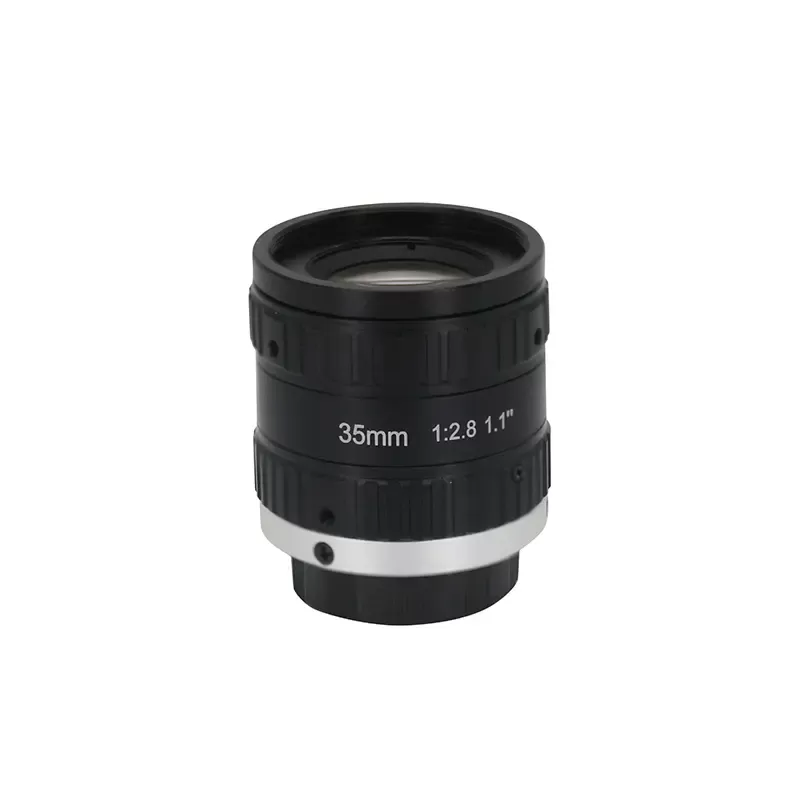
The standard 1-inch sensor format carries nominal dimensions of 13.2 mm horizontally by 8.8 mm vertically, yielding an active diagonal measurement of approximately 15.86 mm. This spatial footprint presents optical constraints distinct from smaller 1/1.8-inch or 2/3-inch architectures. A compatible lens must project an image circle of at least 16.0 mm to prevent optical vignetting and maintain uniform illumination across the outermost corners of the focal plane array.
Pixel pitch directly dictates the required spatial frequency resolution of the imaging lens. The deployment of sensors such as the Sony Pregius series features unit cell dimensions ranging from 3.45 micrometers down to 2.4 micrometers. According to the Nyquist-Shannon sampling theorem, the optical assembly must resolve frequencies matching the sensor cutoff:
For a 3.45-micrometer pixel pitch, the Nyquist frequency corresponds to approximately 145 line pairs per millimeter (lp/mm).
For a 2.4-micrometer pixel pitch, the optical resolving threshold escalates to roughly 208 line pairs per millimeter (lp/mm).
Failing to preserve contrast at these frequencies produces image degradation, rendering high-megapixel sensors ineffective. The optical system must exhibit high Modulation Transfer Function (MTF) values not merely on-axis, but across the full field of view (FOV). High off-axis MTF performance requires sophisticated field flattening and astigmatism correction within the optical train.
Chief Ray Angle (CRA) matching represents another critical parameter. Modern back-illuminated (BSI) and global shutter CMOS sensors incorporate micro-lenses atop each photodiode to redirect incoming light into the silicon substrate. If the exit pupil of the optical system is positioned too close to the image plane, peripheral light rays strike the sensor at steep angles. When the lens CRA deviates substantially from the sensor micro-lens CRA acceptance curve, the vision system suffers from angular shading, micro-lens cross-talk, and peripheral color shifting. Optical designs targeting the 1-inch format must maintain a nearly telecentric or quasi-telecentric configuration on the image side to keep incidence angles within the optimal range of the photodiode collection cones.
Structural Dynamics and Aberration Control in 1 Inch Sensor Camera Lens Design
Correcting optical aberrations across a 16 mm image circle requires a sophisticated element layout. Monochromatic aberrations such as spherical aberration, coma, and field curvature scale aggressively as the clear aperture and focal length increase. Balancing optical speed—typically between f/1.4 and f/2.8—against spatial resolution demands the integration of anomalous partial dispersion glasses and precision-molded aspherical elements.
Chromatic aberrations present distinct challenges across broadband illumination profiles. Axial chromatic aberration causes different wavelengths of light to focus on disparate planes along the optical axis, leading to image softening in multi-spectral or white-light illumination. Lateral chromatic aberration shifts the magnification of different wavelengths across the periphery, introducing color fringing along high-contrast edges. Precision optical manufacturing protocols, such as those implemented by Jinyuan, employ low-dispersion optical glass formulations and computer-optimized air-spaced doublets to converge blue (486 nm), green (587 nm), and red (656 nm) wavelengths onto an identical focal plane.
Geometric distortion control requires equal scrutiny, especially for optical metrology, automated optical inspection (AOI), and spatial mapping. While consumer-grade lenses frequently permit 2% to 5% barrel or pincushion distortion to reduce assembly cost and element count, precision vision demands TV distortion levels constrained below 0.1% to 0.5%. Minimizing distortion optically eliminates the need for computational warping algorithms, which inevitably resample pixels, reduce native MTF, and consume computational cycles on embedded processing units.
Stray light and internal reflections degrade system contrast. Optical assemblies designed for high-resolution 1-inch sensors rely on broadband anti-reflective (BBAR) thin-film coatings deposited via physical vapor deposition (PVD). These multi-layer dielectric coatings suppress surface reflections down to less than 0.5% per glass-air interface across the 400 nm to 700 nm spectrum. Internal mechanical barrels feature micro-grooving, light-absorbing structural baffling, and matte-black anodization to prevent grazing-incidence scatter from compromising dark-field inspection.
Mechanical Architectures and Interface Stability
The mechanical chassis housing a 1 Inch Sensor Camera Lens must exhibit environmental durability while preserving optical alignment within sub-micron tolerances. Operating temperatures in industrial facilities, traffic corridors, and aerial payloads fluctuate widely, inducing thermal expansion and contraction within mechanical assemblies.
Athermalization strategies prevent focus drift across operating envelopes typically spanning -20°C to +60°C. By pairing optical glasses with divergent thermal coefficients of expansion (CTE) alongside specifically selected housing materials—such as aerospace-grade aluminum alloys, brass, or stainless steel—the physical displacement of elements counters the temperature-induced shift in refractive index (dn/dt). This passive athermalization keeps the focal point registered precisely on the sensor surface without active motorized compensation.
Mounting interfaces directly impact alignment reliability. The standard C-mount interface features a 1-inch diameter with 32 threads per inch (1-32 UN) and a nominal flange focal distance of 17.526 mm in air. While the C-mount remains the industrial standard, its physical inner diameter (approximately 25.4 mm) approaches mechanical clearance limits when transmitting optical cones intended for a 16 mm diagonal sensor, particularly at wide focal lengths and wide apertures.
Mechanical Vignetting: Improperly optimized rear element barrels can physically obstruct peripheral rays, casting sharp corner shadows.
Flange Focal Tolerancing: Minor shimming discrepancies or machining variations of ±10 micrometers alter the optical conjugation, severely degrading corner resolution at wide-open apertures.
Vibration Resistance: Industrial machine vision environments subject optics to continuous mechanical vibration. Robust designs feature locking screws for both focus and iris rings, alongside internal adhesive bonding of optical elements to prevent de-centering.
Industrial and Scientific Deployments
The convergence of large sensor formats and high resolving power unlocks new performance tiers across high-throughput industrial and scientific sectors.
Intelligent Transportation Systems (ITS)
Modern traffic enforcement, automated license plate recognition (ALPR), and tolling systems demand multi-lane coverage from a single roadside installation. Standard optical formats often force a compromise between field width and optical detail. A wide-angle 1 Inch Sensor Camera Lens captures multiple highway lanes simultaneously while preserving sufficient pixel density on target vehicles to resolve license plate typography, hazardous material placards, and driver cabin details under high vehicular velocities. The light-gathering advantages of the large optical format enable short exposure times down to 1/1000s without requiring overpowering auxiliary strobes, even in low-ambient twilight conditions.
High-Speed Factory Automation and Semiconductor Inspection
In-line surface mount technology (SMT) inspection and bare-wafer defect detection depend directly on throughput speed and optical contrast. As production lines accelerate, exposure times must decrease to avoid motion blur. Larger pixel sizes afford greater optical electron wells, sustaining low-noise performance during rapid line cycles. The optical assembly must resolve micron-level soldering bridging, cracked silicon edges, and microscopic trace discontinuities across large printed circuit boards. Optical designs from Jinyuan deliver consistent resolving power edge-to-edge, eliminating the false rejects associated with peripheral optical softening.
Biomedical Imaging and Fluorescence Microscopy
Fluorescence microscopy, digital pathology, and cell sorting involve weak optical signals emitted by fluorophores. The light collection efficiency of an optical train scales quadratically with the numerical aperture (NA) and sensor area. A 1-inch format collects substantially more photons per unit time than smaller industrial formats. Lens systems optimized for this discipline must provide elevated transmission efficiencies across extended wavelengths, including the ultraviolet (UV) excitation bands and near-infrared (NIR) emission windows, while suppressing native glass autofluorescence.
Integration Trade-offs: Optical Configurations and Operating Envelopes
Deploying large-format optics requires balancing competing physical parameters. Optical designers must systematically evaluate trade-offs between working distance, depth of field, and optical speed to avoid system-level performance bottlenecks.
The relationship between depth of field (DoF) and optical aperture behaves inversely. Because a 1-inch format demands longer focal lengths than a 2/3-inch format to achieve an identical field of view, the natural depth of field becomes substantially shallower at identical f-numbers. In three-dimensional inspection tasks—such as evaluating connector pin heights or engine block castings—achieving acceptable focus depth necessitates stopping down the aperture to f/5.6 or f/8. Stopping down introduces diffraction limitations. The Airy disk diameter expands according to the formula:
Airy Disk Diameter = 2.44 × λ × N
Where λ is the illumination wavelength and N is the working f-number. At an f-number of f/8 and a standard green wavelength of 550 nm, the central Airy disk diameter reaches approximately 10.7 micrometers. If this optical pattern falls upon a sensor possessing 2.4-micrometer pixels, optical diffraction rather than lens aberrations becomes the governing ceiling of system resolution. System engineers must illuminate targets intensively to operate lenses within their optical sweet spots (typically f/2.8 to f/4.0), rather than stopping down excessively to gain depth of field.
Custom Optical Engineering and Specification Criteria
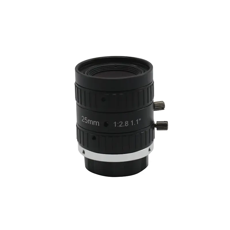
Off-the-shelf catalog optics frequently fall short when projects demand specialized mechanical footprints, extended environmental sealing, or narrow-band spectral performance. Integrating non-standard filter threads, specialized liquid-lens autofocus elements, or ingress protection ratings (such as IP67) necessitates customized optomechanical engineering.
Customization protocols begin with the definition of the operational optical transfer function. Optical engineers model the complete system through ray-tracing software to balance optical prescription parameters against manufacturing yield tolerances. Jinyuan collaborates with system integrators to tailor optical assemblies to exact mechanical envelopes, optimizing back focal distance, spectral transmission profiles, and sensor cover glass thickness compensation. Customizing the anti-reflective thin films to specific laser diode illumination lines (e.g., 405 nm, 635 nm, 850 nm, or 940 nm) elevates signal contrast while mitigating ghosting artifacts that compromise algorithmic edge detection.
Frequently Asked Questions
Why choose a 1 inch sensor camera lens over smaller formats like 2/3-inch or 1/1.8-inch?
A larger optical format provides a broader physical surface area to collect photons. This directly enhances dynamic range, improves low-light performance, and permits higher spatial resolution without reducing pixel size to levels where diffraction severely restricts performance. It is suited for applications requiring high detail across wide fields of view.
How does pixel pitch dictate lens resolving power (lp/mm)?
Pixel pitch determines the spatial Nyquist frequency, which is calculated as 1 / (2 × pixel pitch in millimeters). A sensor with small pixels requires a lens that can deliver high contrast at high line pairs per millimeter. If the lens cannot resolve spatial detail at or near this Nyquist frequency, the resulting image will suffer from blur and loss of high-frequency edge data regardless of the camera megapixel rating.
What causes edge vignetting when deploying a 1-inch format sensor?
Vignetting typically originates from two factors: mechanical vignetting and natural (optical) vignetting. Mechanical vignetting occurs when physical apertures, lens barrels, or improper mounts partially clip off-axis light cones. Optical vignetting follows the cos⁴(θ) law of illumination falloff, where peripheral illumination diminishes relative to field angle. Correcting this requires optical designs with large front elements and controlled chief ray angles.
Can a 1 inch sensor camera lens handle both visible light and SWIR spectra?
Standard visible-light optics are optimized exclusively for the 400 nm to 700 nm range. If deployed within short-wave infrared (SWIR) bands (900 nm to 1700 nm), focal shifts, severe chromatic aberrations, and rapid transmission drops occur due to standard anti-reflective coating reflection and optical glass absorption. Multi-spectral or SWIR imaging requires specialized optical designs featuring custom substrates, unique dispersion characteristics, and dedicated broadband coatings.
How does mechanical locking impact high-vibration machine vision environments?
In environments subject to continuous movement, such as robotic arms or conveyor rails, unsecured focus and aperture rings experience micro-movements over operational cycles. These shifts alter the optical conjugation and exposure consistency. Industrial-grade mechanics incorporate radial or axial locking screws to lock the inner cam barrels securely to the chassis, maintaining calibrated focus and f-stop settings over prolonged use.
What parameters are essential when initiating a custom optical project?
Core integration parameters include sensor specifications (pixel size, active area dimensions, cover glass thickness, and CRA profiles), working distance, required field of view, target magnification, illumination wavelength range, preferred f-number, allowable distortion limits, physical dimensions, and interface mount type.
Initiate Your Optical Engineering Consultation
Precision machine vision and optical metrology require optomechanical systems built precisely to your performance requirements. Whether your architecture demands high-frequency MTF preservation for sub-3-micrometer pixel architectures, specialized environmental sealing, or custom optical coatings, qualified optical engineering guarantees predictable system deployment.
Submit your optical specification sheets, dimensional constraints, and sensor integration requirements to our optical engineering group for a formal technical review and manufacturing feasibility analysis.