

As automated optical inspection (AOI) and industrial metrology advance toward micrometer-level precision, engineers face a complex physics challenge: balancing pixel resolution with light-gathering capability. Shrinking pixel sizes to fit higher resolutions onto standard optical formats inevitably reduces the full well capacity (FWC) of each photodiode, thereby lowering the signal-to-noise ratio (SNR) and compromising dynamic range. Solving this demands an expanded physical footprint, often found by adopting the 1.1" Image Sensor, which provides the necessary surface area to accommodate high-megapixel arrays while maintaining optimal pixel pitch.
Implementing this specific optical format is not merely a matter of upgrading a camera module. It requires a fundamental re-evaluation of the entire optical path, from lens mount mechanics to chief ray angle alignment and thermal dissipation. The following analysis explores the technical nuances of deploying large-target formats in rigorous B2B industrial environments.
1. Understanding the Physics of Pixel Pitch and Full Well Capacity
The primary engineering motivation for increasing the diagonal measurement of a silicon detector is to preserve photon-collection efficiency at high spatial resolutions. When industrial requirements dictate resolutions exceeding 12 megapixels, maintaining a pixel pitch of 3.45 µm or larger is vital for industrial low-light performance.
Quantum Efficiency (QE): Larger pixels present a broader target for incident photons, resulting in higher quantum efficiency across the visible and near-infrared (NIR) spectrums.
Shot Noise Limitation: By increasing the full well capacity—the maximum number of photoelectrons a single pixel can hold before saturation—the detector inherently improves its shot noise characteristics.
Dynamic Range: A broader well capacity combined with low readout noise allows vision systems to capture both highly reflective metal surfaces and deep shadows in a single exposure without clipping data.
2. Resolving Chief Ray Angle (CRA) Mismatch in Large Targets
One of the most complex optical challenges encountered in machine vision is chief ray angle (CRA) mismatch. Micro-lenses are manufactured over each pixel array to focus incident light onto the active silicon area. These micro-lenses are shifted slightly toward the edges of the detector to accommodate the natural angle of light arriving from the objective lens.
When pairing lenses with a 1.1" Image Sensor, engineers must account for the specific CRA profile of the detector. If the lens's exit pupil distance produces an incident light angle steeper than the micro-lenses can accept, severe optical degradation occurs:
Optical Crosstalk: Photons strike adjacent photodiodes, blurring sharp edges and corrupting color fidelity in Bayer-pattern arrays.
Relative Illumination Drop: The edges of the image become significantly darker than the center, a phenomenon often incorrectly attributed solely to mechanical vignetting.
Overcoming this requires specialized telecentric or highly corrected entocentric lens designs. Expert manufacturers like Jinyuan understand that manipulating the exit pupil position during the optical engineering phase is paramount to ensuring uniform light distribution across a 17.6mm diagonal surface.
3. Mitigating Optical Aberrations at the Periphery
As the target diameter increases, light rays traveling to the corners of the detector must pass through the outer edges of the lens elements. This introduces a high susceptibility to various optical aberrations that degrade the Modulation Transfer Function (MTF) at the image periphery.
Spherical and Chromatic Aberration
Spherical aberration occurs because light passing through the edge of a spherical lens focuses at a different point than light passing through the center. To resolve this for large-format targets, optical designers utilize precision-molded aspherical glass elements, which flatten the focal plane and ensure edge-to-edge sharpness. Furthermore, lateral chromatic aberration—where different wavelengths of light magnify differently—must be corrected using anomalous dispersion glass, preventing color fringing on high-contrast edges.
Distortion Control
For metrology applications requiring sub-pixel measurement accuracy, geometric distortion (barrel or pincushion) must be kept near zero. While software calibration can correct distortion mathematically, it inevitably interpolates pixels, reducing the true optical resolution. High-end optical design prioritizes correcting distortion physically within the glass assembly, preserving spatial data integrity.
4. Application Scenarios Demanding Expanded Optical Formats
The transition to larger optical architectures is driven strictly by industrial application requirements where traditional 1-inch or 2/3-inch formats fall short.
Automated Optical Inspection (AOI) in Semiconductor Manufacturing
In wafer-level packaging and printed circuit board (PCB) inspection, the system must detect defects measuring only a few micrometers. Utilizing a high-resolution array allows the inspection machinery to capture a wider field of view (FOV) per frame. This reduces the number of mechanical movements required by the XY-gantry system, drastically increasing the throughput of the production line.
High-Speed Intelligent Transportation Systems (ITS)
Modern highway monitoring requires reading license plates and recognizing vehicle characteristics across three or four lanes simultaneously. This demands an expansive FOV. Furthermore, capturing vehicles moving at high velocities requires global shutter architecture combined with a 1.1" Image Sensor to capture fast-moving targets without the focal plane distortion (jello effect) inherent to rolling shutter mechanisms. The larger format allows for high light-gathering capability even at extremely short exposure times (e.g., 1/5000th of a second).
5. Thermal Management and Mechanical Integration
High-resolution global shutter arrays outputting data at 60 to 100 frames per second generate immense data bandwidth. Transmission protocols such as 10GigE, CoaXPress 2.0, or Camera Link process gigabits of data per second, producing substantial heat within the camera housing.
Dark Current and Thermal Noise
In semiconductor physics, dark current roughly doubles for every 5 to 8 degrees Celsius increase in junction temperature. If the heat generated by the Analog-to-Digital Converters (ADC) and the FPGA is not properly dissipated, thermal noise will flood the photodiodes, drastically reducing the SNR. Effective camera designs incorporate robust thermal coupling, transferring heat from the detector board directly to the outer metallic chassis via specialized thermal interface materials (TIM).
Opto-Mechanical Stability
Thermal expansion affects the metal housing and the lens barrel. As temperatures fluctuate in industrial environments, the flange focal distance can shift, causing the system to lose focus. Utilizing precision-engineered mounts and lens barrels from Jinyuan ensures that the coefficient of thermal expansion (CTE) is tightly controlled, maintaining stable optical alignment across extreme temperature gradients.
6. Navigating Lens Mount Limitations
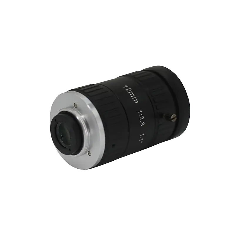
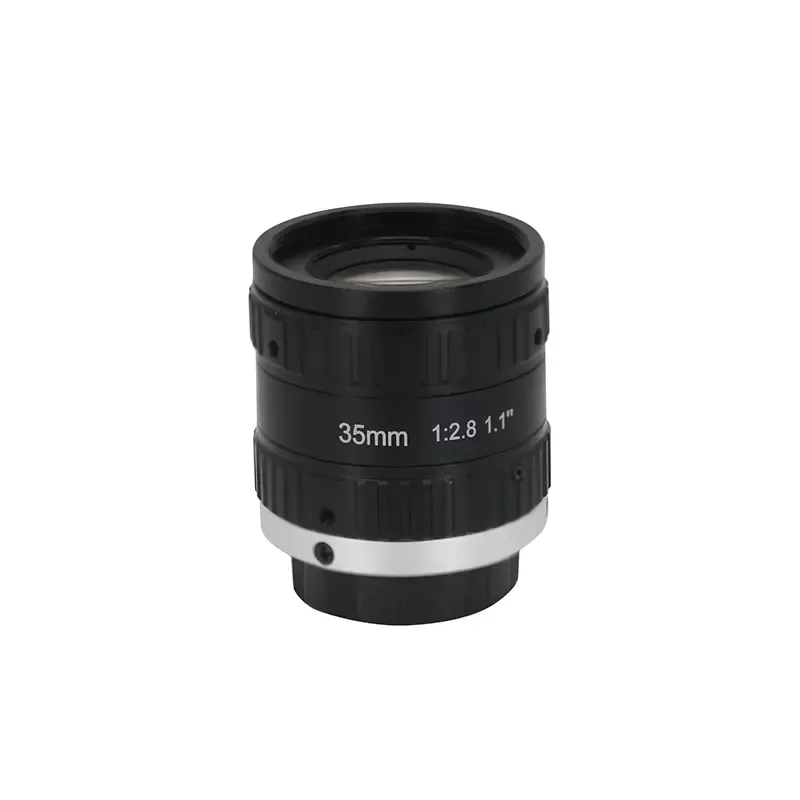
A significant physical constraint in adopting larger formats lies in the lens mount standard. The ubiquitous C-mount specifies a thread diameter of 1 inch (25.4mm) with a flange focal distance of 17.526mm. Because a 17.6mm diagonal detector is mathematically very close to the inner physical diameter of the C-mount thread, light rays targeting the extreme corners can be mechanically clipped by the rear aperture of the lens barrel.
To prevent mechanical vignetting, vision engineers must either select highly specialized C-mount lenses designed specifically with protruding rear elements to bypass the thread bottleneck, or transition to larger industrial mounts. Formats such as the M42 mount, T-mount, or F-mount provide ample physical clearance, ensuring that the light cone remains completely unobstructed as it travels to the detector corners.
7. The Role of MTF in Large Format System Design
Modulation Transfer Function (MTF) is the definitive metric for quantifying how well an optical system transfers contrast from the subject to the image plane at varying spatial frequencies (measured in line pairs per millimeter, or lp/mm). When evaluating lenses for large-format arrays, a single center MTF reading is insufficient.
Engineers must analyze the MTF curve across the entire 8.8mm radius (the distance from the center to the corner of the target). A high-performance lens will exhibit an MTF curve that remains relatively flat from the center to the periphery, indicating uniform resolving power. If the MTF drops sharply beyond the 5mm radius mark, the resulting image will suffer from soft corners, rendering edge data useless for precise metrology algorithms.
Frequently Asked Questions (FAQ)
Q1: What exactly defines the diagonal measurement of the 1.1" Image Sensor?
A1: The terminology originates from the era of vidicon cathode-ray tubes. The "inch" measurement refers to the outer diameter of the glass vacuum tube, not the active diagonal of the silicon. For this specific format, the actual active diagonal of the silicon detector typically measures approximately 17.6mm.
Q2: How does relative illumination impact defect detection algorithms?
A2: Relative illumination refers to the brightness at the corners of an image compared to the center (which is 100%). If a lens provides only 40% relative illumination at the edges, the corners will appear dark. While software flat-field correction can artificially boost the brightness, it simultaneously amplifies the noise in those regions, which can trick defect detection algorithms into identifying false positives.
Q3: Why is global shutter architecture preferred over rolling shutter in industrial inspection?
A3: A rolling shutter exposes rows of pixels sequentially. If the inspected object is moving rapidly on a conveyor belt, the object will shift position between the time the first row and the last row are exposed, causing geometric distortion. A global shutter exposes every photodiode simultaneously, freezing high-speed motion with perfect spatial geometry.
Q4: Can I use a standard 1-inch lens on a 17.6mm diagonal target?
A4: It is highly discouraged. A standard 1-inch lens is designed to cast an image circle of 16mm. Projecting a 16mm image circle onto a 17.6mm diagonal detector will result in heavy mechanical vignetting, meaning the extreme corners of the resulting image will be completely black, wasting the resolution of the detector.
Q5: What is the significance of anomalous dispersion glass in large format lenses?
A5: Anomalous dispersion glass possesses unique refractive properties that differ from standard optical glass. It is utilized to precisely correct secondary spectrum chromatic aberrations. In large-target optics, where light rays bend at steeper angles at the periphery, this specialized glass ensures that red, green, and blue wavelengths converge at the exact same focal point, eliminating color fringing.
Advancing machine vision capabilities beyond standard definitions necessitates a rigorous approach to physical optical formats. The decision to integrate a broader pixel array is a fundamental engineering shift that impacts photon collection, thermal dynamics, and spatial resolution. Successfully deploying a 1.1" Image Sensor requires meticulous optical matching to overcome peripheral aberrations, strict adherence to MTF requirements, and the correct mechanical mounts to prevent data loss at the image corners.
For automated inspection systems to perform reliably at high throughputs, off-the-shelf optics are rarely sufficient. Precision alignment, controlled relative illumination, and zero-distortion glass elements are the foundations of modern metrology.
If your engineering team is currently designing a high-resolution machine vision system and requires precision optical matching, expert guidance is paramount. Reach out to the technical team at Jinyuan to discuss custom lens designs, aberration control, and optimal mechanical integration for your specific application. Send us a detailed B2B Inquiry today to ensure your next automated optical inspection system achieves maximum optical fidelity.

